
Introduction
Hello. In this short article I am going to take you through my design approach on the homemade cubesat onboard computer, which I shall call OBC from now on.
The OBC is basically the brains of the whole cubesat. It aggregates all data from other PCBs and does the processing as well as decision making to control and manage the cubesat. As well as the functions below:
- Telemetry data management
- System housekeeping
- On board time synchronization
- Failure detection
- Failure isolation
- System recovery
My design philosophy for Project Shadow flight was such that the OBC would receive as much processed data as possible from other boards so as to lower its processing time and load.
Note that all the components used in this design are not radiation-hardened due to cost implications.
Design approach
Project’s shadow flight OBC is composed of the following major parts:
- STM32 microcontroller
- User LED and button
- Programing and debug header
- Dedicated power regulator
- External watchdog timer
- USB-C debug port
- External brown-out detector circuit
- Debug LEDs
- SD card for data storage
- 16MB external SPI flash memory
- 64KB EEPROM
- Real-Time Clock circuit
- ISA connector
The schematic is shown below (NB: this schematic might be a little bit different from the complete version at the time of writing)
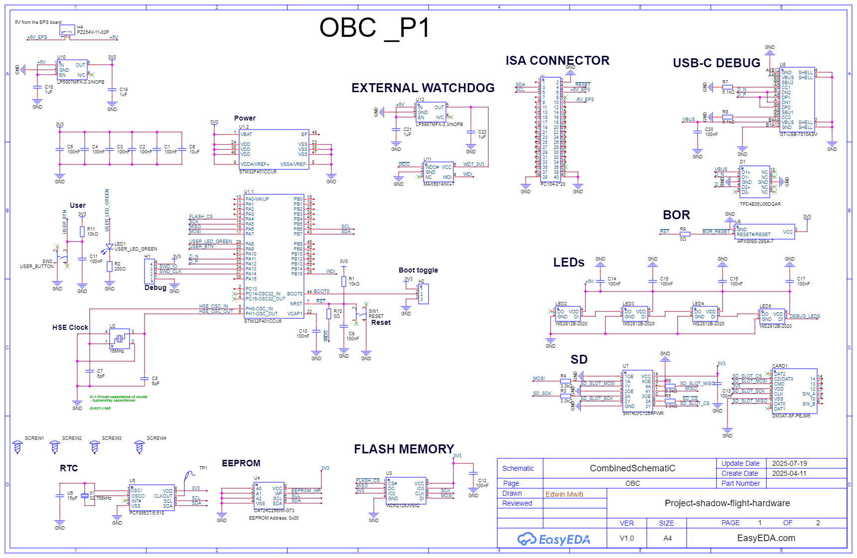
Schematic deconstruction
1. STM32 MCU
I chose to use the STM32 series of chips for the microcontroller unit. This is a 32 bit MCU with such superior qualities compared to 8-bit or 16-bit MCUs. I chose this because of its processing speed and versatility. Plus if you are going to design a budget friendly cubesat, I believe you can never go wrong with an STM32.
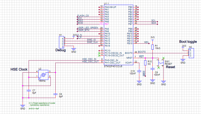
The specific MCU used here is the STM32F401CCU6. One reason is that it has sufficient pin count to handle all my peripherals. Also I had several of them lying around so that would cut my prototyping time by half. These is a summary of its features:
- 1.7V to 3.6V power supply
- Arm 32-bit Cortex -M4 CPU with an FPU
- Up to 84MHz clock speed
- Up to 256KB of flash memory
- 64KB of SRAM
- Inbuilt POR, BOR, PDR and PVD
- 4-26MHz crystal oscillator
- 11 comms interfaces (UART, SPI etc)
- Up to 11 timers etc
This is just but a summary of its features. You can read more about this specific here: (https://www.st.com/en/microcontrollers-microprocessors/stm32f401cc.html)
Otherwise it is a sufficient MCU to use for this case. As seen from the above schematic, I have designed the surrounding schematic to make the MCU boot as required. This includes a high-speed external 16MHz crystal, boot and reset circuitry and the debug header. These circuits will be sufficient to boot the MCU fully.
2. User LED and User button
What other way to confirm the MCU is working other than LEDs? This is one of the methods used to debug hardware. I added one external LED so that when I first boot the MCU, I can blink these LED to confirm my code is running well before everything else.
Also, to test GPIO input, I added a tactile push button for processing user inputs etc. Plus my thinking is that it can be repurposed to handle something else, on ground of course, because no one is going to be pressing buttons in space.
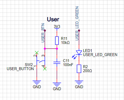
Pretty simple but handy when debugging hardware.
3. Programming and debug header
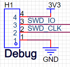
This circuit is nothing but the header pins used to program the STM32 MCU via Serial Wire Debug (SWD) pins. They are a combination of 3V3, GND, SWDIO and SCLK. It will be used to upload the firmware to the MCU.
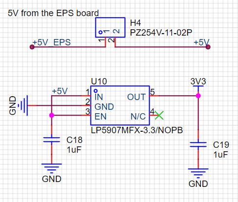
4. Dedicated power regulator
The MCU cannot obviously run without a power supply. Power is supplied from the Electrical Power Supply (EPS) board, which I am going to write a future design article on.
This power comes as 5V from the EPS, but the MCU requires 3.3V. So I added a dedicated 3.3V regulator on the OBC board.
Why am I calling it dedicated though? There are 2 ways to supply power to such a subsystem: Distributed architecture or Centralized architecture.
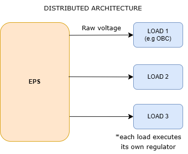
a) Distributed architecture
In this approach, raw voltage is supplied from the EPS board. The subsystem that receives it is responsible for regulating it. This is the approach I used. The advantage I figured is that we have a failure point that is singled out. What I mean is that in case the OBC fails to receive 3.3V, I will know where to start debugging the power. Another advantage is that carrying 5V is better in handling voltage voltage drops along the way than it is carrying 3.3V.
This illustration explains this architecture:
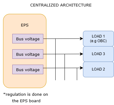
b) Centralized architecture
This is the opposite of distributed architecture. Here the supply voltage is regulated on the EPS and specific bus voltages are sent to the loads. So if I were to use this I would regulate the 5V power on the EPS and send 3.3V from the EPS to the OBC.
This is illustrated below:
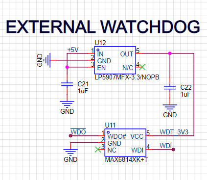
5. External watchdog timer (WDT)
Think about this. What happens when a possible firmware bug causes the cubesat firmware to hang indefinitely, in space? If we were on ground, we would easily notice this and press the reset button. But in space, where conditions do not allow, we need a mechanism to reset the software when the system hangs.
This is the role of the watchdog timer. To detect a possible hang and reset the software. The basic operation of a watchdog timer is that it is automatically reset by the software during normal operation, so it does not expire.
If the system fails to reset the timer due to a freeze or a crash or an infinite loop, the watchdog expires. Once it expires, the watchdog timer triggers a system reset or corrective action to restore normal operation.
Now, there are 2 ways to implement a watchdog: internal (software based) or external. Both work fine, and I will use both in this case but what happens if the CPU fails? You got it - The software timer will fail too. So I decided to have an external WDT to increase system robustness.
The IC used here is the MAX6814 from analog devices. It simply monitors the system for software code execution errors. Datasheet here for more info: (https://www.analog.com/media/en/technical-documentation/data-sheets/MAX6814.pdf)
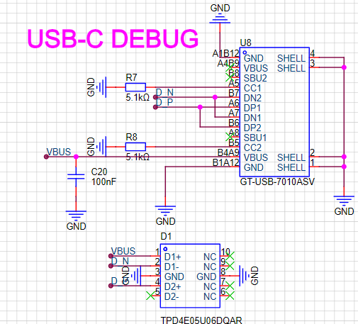
6. USB-C debug port
This part is used as a debug port to send messages via USB to an external PC etc. It can also be used as a programming channel in case the SWD fails or as a secondary programming channel. This circuit is pretty simple following the normal design standard. An ESD protection diode is also included to flash out high voltage spikes and noise.
7. External brown-out detector circuit
Brown-outs. Classic failures on most systems. A brown-out is simply a situation where the voltage needed by a component goes below the minimum accepted voltage, causing the component to misbehave or fail to operate all together. What we want is a known voltage level on any component.
So what do we do? We reset the system in case the system voltage goes below a given threshold. This is where the BOR circuit comes in handy. STM32 implements an internal BOR but again for robustness I implement an external BOR circuit.
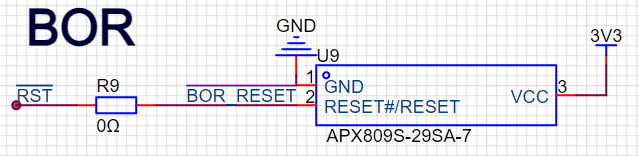
This circuit asserts the RESET line on the MCU if the voltage goes below 2.9V. See datasheet for more:
(https://www.mouser.com/datasheet/2/115/DIOD_S_A0007666380_1-2543067.pdf?srsltid=AfmBOooYNw8QktCWNU6XURc0l-4tPovOsjjTUpPxpAnihCiBYzZ7Swu5)
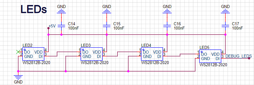
8. Debug LEDs
I decided to add 4 addressable LEDs to indicate STATES during development. I will basically be lighting up different LEDs based on a specific state. This allows me to easily visually inspect the operation of the software during development.
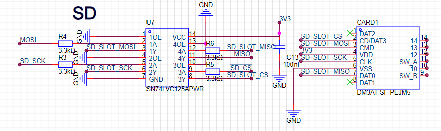
9. SD card
Where to store flight log data, SD card. Because it has a larger storage density and space for a cheaper price. I think the best place to explain this subsystem will be on the software side. But for now here is the circuit. By the way this is the circuit found on common SD card modules, featuring a bidirectional buffer and the SD card slot, and SPI interface.
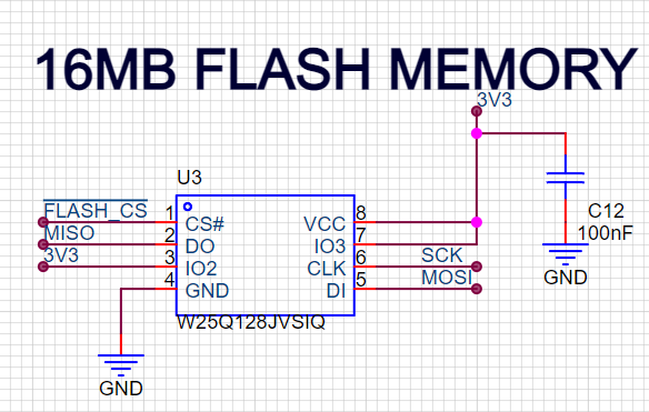
10. 16MB Flash memory
To store small data files e.g config files, cubesat health status, can be used to log system events e.g errors and operational logs, will allow for OTA reprogramming etc.
11. 64KB EEPROM
Remember our BOR and watchdog circuits above, what happens when we reset the system? Does the cubesat start from the beginning again? No. It should restore itself to the last known state after reset. And this STATEis stored in the EEPROM.
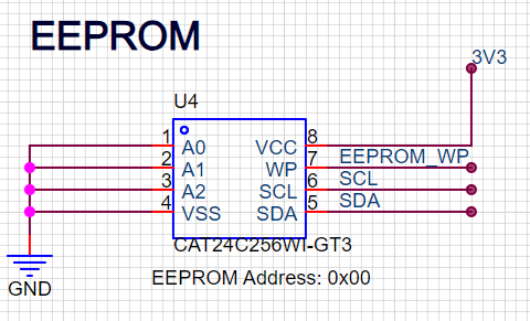
Since the EEPROM is low memory, I will also use it to store the satellite ID, Operational modes, mission parameters e.g calibration data and communication frequencies etc.
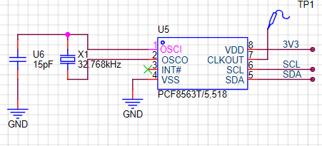
12. Real Time Clock
Real time clocks have one use and one use only in this case. Keep track of time in case the main clock goes off.
13. ISA connector
This connector is used to couple the OBC board to other PCBs using the PC/104 cubesat standard. I will discuss it in a later article.
Conclusion
And there you have it. A peek into my cubesat’s brain, and the components that bring it to life. If you are curious to dive deeper or you just love tech space as much as I do, you can check out the full project here: (https://github.com/bytecod3/Project-Shadow-Flight). I will be posting updates on design progress there.
Until next time, keep your eyes to the stars.
Blog image credits: Clyde space: https://www.aac-clyde.space/what-we-do/space-products-components/command-data-handling/kryten-m3